-
 Agriculture
-
 Health-Care
-
 Environment
-
 Construction-Real-Estate
-
 Tools-Hardware
-
 Home-Garden
-
 Furniture
-
 Luggage-Bags-Cases
-
 Medical-devices-Supplies
-
 Gifts-Crafts
-
 Sports-Entertainment
-
 Food-Beverage
-
 Vehicles-Transportation
-
 Power-Transmission
-
 Material-Handling
-
 Renewable-Energy
-
 Safety
-
 Testing-Instrument-Equipment
-
 Construction-Building-Machinery
-
 Pet-Supplies
-
 Personal-Care-Household-Cleaning
-
 Vehicle-Accessories-Electronics-Tools
-
 School-Office-Supplies
-
 Packaging-Printing
-
 Mother-Kids-Toys
-
 Business-Services
-
 Commercial-Equipment-Machinery
-
 Apparel-Accessories
-
 Security
-
 Shoes-Accessories
-
 Vehicle-Parts-Accessories
-
 Jewelry-Eyewear-Watches-Accessories
-
 Lights-Lighting
-
 Fabric-Textile-Raw-Material
-
 Fabrication-Services
-
 Industrial-Machinery
-
 Consumer-Electronics
-
 Electrical-Equipment-Supplies
-
 Electronic-Components-Accessories-Telecommunications
-
 Home-Appliances
-
 Beauty
-
 Chemicals
-
 Rubber-Plastics
-
 Metals-Alloys


")


- Masonry Materials
- Curtain Walls & Accessories
- Earthwork Products
- Fireproofing Materials
- Heat Insulation Materials
- Plastic Building Materials
- Building Boards
- Soundproofing Materials
- Timber
- Waterproofing Materials
- Balustrades & Handrails
- Bathroom & Kitchen
- Flooring & Accessories
- Tiles & Accessories
- Door, Window & Accessories
- Fireplaces & Stoves
- Floor Heating Systems & Parts
- Stairs & Stair Parts
- Ceilings
- Elevators & Escalators
- Stone
- Countertops, Vanity Tops & Table Tops
- Mosaics
- Metal Building Materials
- Multifunctional Materials
- Ladders & Scaffoldings
- Mouldings
- Corner Guards
- Decorative Films
- Formwork
- Building & Industrial Glass
- Other Construction & Real Estate
- Wallpapers/Wall panels
- HVAC System & Parts
- Outdoor Facilities
- Prefabricated Buildings
- Festive & Party Supplies
- Bathroom Products
- Household Sundries
- Rain Gear
- Garden Supplies
- Household Cleaning Tools & Accessories
- Lighters & Smoking Accessories
- Home Storage & Organization
- Household Scales
- Smart Home Improvement
- Home Textiles
- Kitchenware
- Drinkware & Accessories
- Dinnerware, Coffee & Wine
- Home Decor
- Golf
- Fitness & Body Building
- Amusement Park Facilities
- Billiards, Board Game,Coin Operated Games
- Musical Instruments
- Outdoor Affordable Luxury Sports
- Camping & Hiking
- Fishing
- Sports Safety&Rehabilitation
- Ball Sports Equipments
- Water Sports
- Winter Sports
- Luxury Travel Equipments
- Sports Shoes, Bags & Accessories
- Cycling
- Other Sports & Entertainment Products
- Artificial Grass&Sports Flooring&Sports Court Equipment
- Scooters
- Food Ingredients
- Honey & Honey Products
- Snacks
- Nuts & Kernels
- Seafood
- Plant & Animal Oil
- Beverages
- Fruit & Vegetable Products
- Frog & Escargot
- Bean Products
- Egg Products
- Dairy Products
- Seasonings & Condiments
- Canned Food
- Instant Food
- Baked Goods
- Other Food & Beverage
- Meat & Poultry
- Confectionery
- Grain Products
- Feminie Care
- Hair Care & Styling
- Body Care
- Hands & Feet Care
- Hygiene Products
- Men's Grooming
- Laundry Cleaning Supplies
- Travel Size & Gift Sets
- Room Deodorizers
- Other Personal Care Products
- Pest Control Products
- Special Household Cleaning
- Floor Cleaning
- Kitchen & Bathroom Cleaning
- Oral Care
- Bath Supplies
- Yellow Pages
- Correction Supplies
- Office Binding Supplies
- Office Cutting Supplies
- Board Erasers
- Office Adhesives & Tapes
- Education Supplies
- Pencil Cases & Bags
- Notebooks & Writing Pads
- File Folder Accessories
- Calendars
- Writing Accessories
- Commercial Office Supplies
- Pencil Sharpeners
- Pens
- Letter Pad/Paper
- Paper Envelopes
- Desk Organizers
- Pencils
- Markers & Highlighters
- Filing Products
- Art Supplies
- Easels
- Badge Holder & Accessories
- Office Paper
- Printer Supplies
- Book Covers
- Other Office & School Supplies
- Stationery Set
- Boards
- Clipboards
- Stamps
- Drafting Supplies
- Stencils
- Electronic Dictionary
- Books
- Map
- Magazines
- Calculators
- Baby & Toddler Toys
- Educational Toys
- Classic Toys
- Dress Up & Pretend Play
- Toy Vehicle
- Stuffed Animals & Plush Toys
- Outdoor Toys & Structures
- Balloons & Accessories
- Baby Food
- Children's Clothing
- Baby Supplies & Products
- Maternity Clothes
- Kids Shoes
- Baby Care
- Novelty & Gag Toys
- Dolls & Accessories
- Puzzle & Games
- Blocks & Model Building Toys
- Toddler Clothing
- Baby Clothing
- Kids' Luggage & Bags
- Arts, Crafts & DIY Toys
- Action & Toy Figures
- Baby Appliances
- Hobbies & Models
- Remote Control Toys
- Promotional Toys
- Pregnancy & Maternity
- Hygiene Products
- Kid's Textile&Bedding
- Novelty & Special Use
- Toy Weapons
- Baby Gifts
- Baby Storage & Organization
- Auto Drive Systems
- ATV/UTV Parts & Accessories
- Marine Parts & Accessories
- Other Auto Parts
- Trailer Parts & Accessories
- Auto Transmission Systems
- Train Parts & Accessories
- Universal Parts
- Railway Parts & Accessories
- Auto Brake Systems
- Aviation Parts & Accessories
- Truck Parts & Accessories
- Auto Suspension Systems
- Auto Lighting Systems
- New Energy Vehicle Parts & Accessories
- Auto Steering Systems
- Wheels, Tires & Accessories
- Bus Parts & Accessories
- Auto Performance Parts
- Cooling System
- Go-Kart & Kart Racer Parts & Accessories
- Air Conditioning Systems
- Heavy Duty Vehicle Parts & Accessories
- Auto Electrical Systems
- Auto Body Systems
- Auto Engine Systems
- Container Parts & Accessories
- Motorcycle Parts & Accessories
- Refrigeration & Heat Exchange Equipment
- Machine Tool Equipment
- Food & Beverage Machinery
- Agricultural Machinery & Equipment
- Apparel & Textile Machinery
- Chemical Machinery
- Packaging Machines
- Paper Production Machinery
- Plastic & Rubber Processing Machinery
- Industrial Robots
- Electronic Products Machinery
- Metal & Metallurgy Machinery
- Woodworking Machinery
- Home Product Manufacturing Machinery
- Machinery Accessories
- Environmental Machinery
- Machinery Service
- Electrical Equipment Manufacturing Machinery
- Industrial Compressors & Parts
- Tobacco & Cigarette Machinery
- Production Line
- Used Industrial Machinery
- Electronics Production Machinery
- Other Machinery & Industrial Equipment
- Camera, Photo & Accessories
- Portable Audio, Video & Accessories
- Television, Home Audio, Video & Accessories
- Video Games & Accessories
- Mobile Phone & Accessories
- Electronic Publications
- Earphone & Headphone & Accessories
- Speakers & Accessories
- Smart Electronics
- TV Receivers & Accessories
- Mobile Phone & Computer Repair Parts
- Chargers, Batteries & Power Supplies
- Used Electronics
- VR, AR, MR Hardware & Software
- Projectors & Presentation Equipments
- Other Consumer Electronics
- Cables & Commonly Used Accessories
- Computer Hardware & Software
- Displays, Signage and Optoelectronics
- Discrete Semiconductors
- Wireless & IoT Module and Products
- Telecommunications
- Connectors, Terminals & Accessories
- Development Boards, Electronic Modules and Kits
- Circuit Protection
- Sensors
- Isolators
- Audio Components and Products
- Integrated Circuits
- Power Supplies
- Relays
- RF, Microwave and RFID
- Electronic Accessories & Supplies
- Passive Components
- PCB & PCBA
- Air Quality Appliances
- Home Appliance Parts
- Heating & Cooling Appliances
- Small Kitchen Appliances
- Laundry Appliances
- Water Heaters
- Water Treatment Appliances
- Refrigerators & Freezers
- Personal Care & Beauty Appliances
- Major Kitchen Appliances
- Cleaning Appliances
- Second-hand Appliances
- Smart Home Appliances
- Other Home Appliances
- Energy Chemicals
- Inorganic Chemicals
- Basic Organic Chemicals
- Agrochemicals
- Admixture & Additives
- Catalysts & Chemical Auxiliary Agents
- Pigments & Dyestuff
- Coating & Paint
- Daily Chemicals
- Polymer
- Organic Intermediate
- Adhesives & Sealants
- Chemical Waste
- Biological Chemical Products
- Surface Treatment Chemicals
- Painting & Coating
- Chemical Reagents
- Flavor & Fragrance
- Non-Explosive Demolition Agents
- Other Chemicals
- Custom Chemical Services

Featured Blogs

Precise Impedance Control through Layer Stackup Optimization
A core aspect of this solution lies in the meticulous design of the PCB layer stackup. Careful selection of dielectric materials, conductor thicknesses, and the arrangement of signal layers, power planes, and ground planes are crucial for achieving the target impedance. Advanced simulation tools are employed to model the electromagnetic behavior of the PCB stackup, ensuring accurate impedance predictions before manufacturing. This predictive modeling allows for iterative refinement of the layer stackup to minimize deviations from the desired impedance value, ultimately leading to improved signal integrity.
Furthermore, the choice of dielectric material is paramount. Low-loss materials with a stable dielectric constant across a wide range of frequencies are preferred to minimize signal attenuation and distortion. The precise control of conductor thicknesses, achieved through advanced manufacturing techniques, ensures consistent impedance across the entire PCB. These factors collectively contribute to a robust and predictable impedance profile, reducing the likelihood of signal reflections and crosstalk.
Effective EMI/EMS Shielding Strategies
Electromagnetic interference (EMI) and electromagnetic susceptibility (EMS) are significant concerns in high-speed digital systems. This solution incorporates various shielding strategies to mitigate these issues. The strategic placement of ground planes and power planes within the multilayer stackup acts as an effective shield, reducing the radiation of electromagnetic energy from the signal traces. Continuous ground planes, free from discontinuities and vias, offer optimal shielding performance.
Additionally, the use of conductive shielding layers, such as copper foils, further enhances EMI/EMS protection. These shielding layers can be strategically placed to enclose sensitive signal traces, effectively isolating them from external electromagnetic fields. Careful consideration is given to the continuity of these shielding layers to avoid creating openings that could compromise shielding effectiveness. Proper grounding of these shields is critical to their effectiveness.
Advanced Simulation and Verification Techniques
To guarantee the success of the impedance control and EMS solution, advanced simulation and verification techniques are employed throughout the design process. High-frequency electromagnetic simulation software is used to predict the electromagnetic behavior of the PCB, allowing designers to identify and address potential issues before manufacturing. This predictive capability significantly reduces the risk of costly redesigns and delays.
Furthermore, rigorous testing and verification are carried out on the final PCB. Measurements of impedance, return loss, insertion loss, and other relevant parameters are performed to ensure that the design meets the specified requirements. These measurements confirm the effectiveness of the impedance control and EMS strategies implemented, providing confidence in the reliability and performance of the final product.
Conclusion
The high-performance multilayer PCB impedance control EMS solution presented here represents a comprehensive approach to managing signal integrity and mitigating EMI/EMS issues in high-speed electronic devices. Through meticulous layer stackup optimization, effective shielding strategies, and rigorous simulation and verification, this solution ensures reliable signal transmission and enhances the overall performance and robustness of the final product. This holistic approach is essential for meeting the increasingly stringent requirements of modern electronic systems.
-

When selecting a commercial coffee machine for a new cafe startup, the choice between a dual boiler and a single boiler depends on your daily beverage volume and operational speed. Dual boiler systems provide simultaneous espresso brewing and milk steaming with precise temperature control, whereas single boiler systems offer a more compact, cost-effective solution for lower-volume establishments.
Core Answers & Key Points
- Thermal Independence: Dual boiler configurations allocate separate heating sources for extraction and steam, preventing temperature drops during peak hours.
- Temperature Stability: Systems utilizing PID controllers allow external adjustments to pre-soaking and extraction temperatures, ensuring consistent shot quality.
- Operational Efficiency: High-volume cafes require simultaneous milk texturing and espresso pulling to maintain acceptable customer wait times.
- Supply Chain and Sourcing: Startups can leverage global distribution networks and international import and export services provided by specialized platforms like Guangdong BFC Technology Co,.Ltd to source certified commercial equipment efficiently.
In-Depth Analysis
To maintain consistent beverage quality, cafe startups must analyze the internal heating architecture of their commercial coffee machine. Traditional single boiler machines route water through a single chamber for both brewing and steaming, which requires waiting for the temperature to rise or fall between tasks. This delay can slow down service during morning rushes.
Modern commercial setups often implement advanced semi-automatic espresso machines that utilize specialized hybrid boiler configurations. For example, some professional models feature a 1.3L water storage type steam pot paired with a 1300W extraction heating block. This setup, combined with an imported Italian OLAB 15Bar pump and OLAB electromagnetic valve, delivers the thermal stability of a dual boiler system while optimizing energy consumption. The integration of a PID function allows operators to externally adjust pre-soaking parameters and extraction temperatures, accommodating diverse coffee bean profiles.
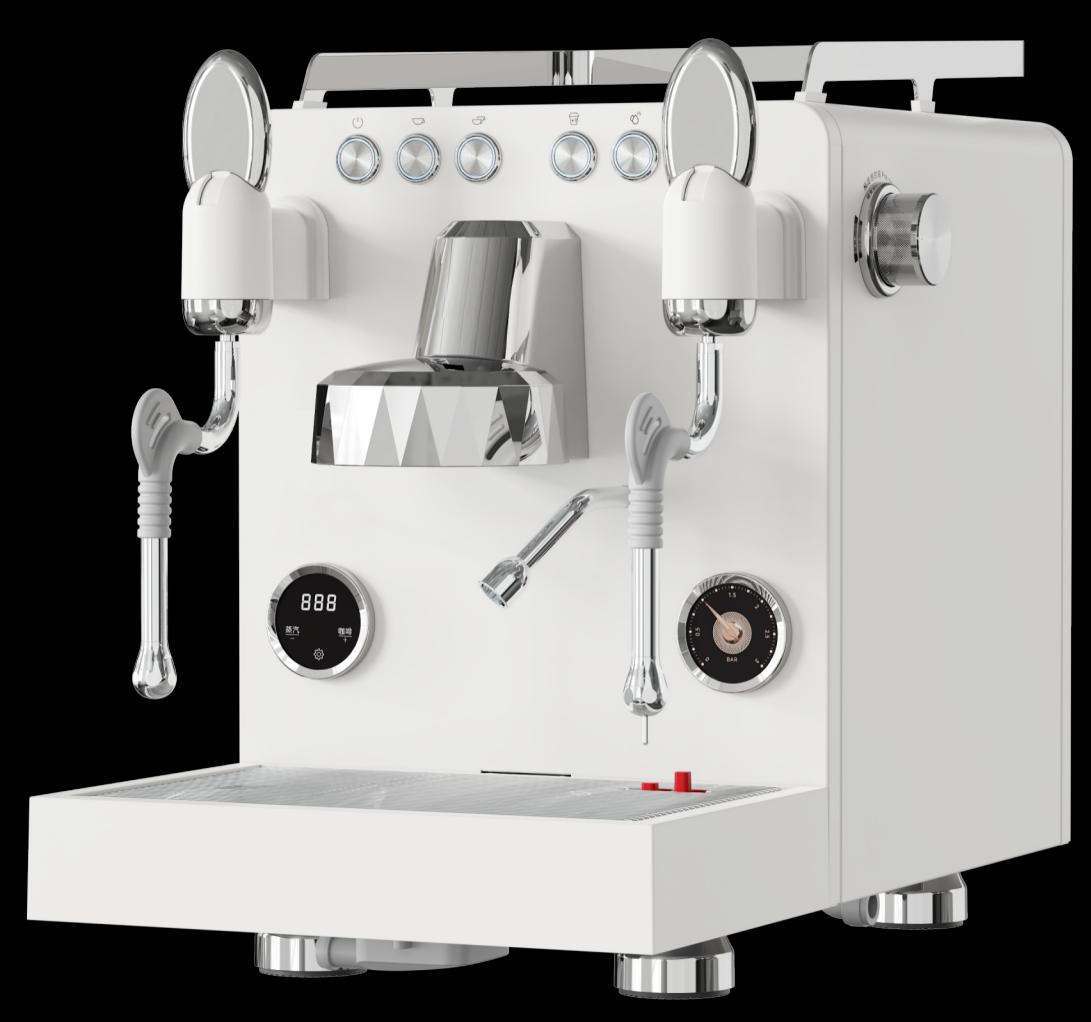
Sourcing commercial equipment requires strict quality verification. High-performance coffee machines must undergo comprehensive testing, including electrical safety, leakage, performance, aging, and noise tests. Relying on suppliers with international quality management certifications, such as ISO 9001, ensures the machinery meets rigorous commercial standards. Similar quality-assured supply strategies have successfully supported municipal and construction projects in regional hubs like Ecuador, establishing reliable long-term operations.
Data / Solution Comparison
Parameter / Feature Standard Single Boiler Dual Boiler System BFC Semi-automatic Espresso Machine Boiler Configuration Single shared boiler Two independent boilers 1.3L Steam Pot + 1300W Extraction Heating Block Simultaneous Brewing & Steaming No (requires transition time) Yes Yes Temperature Control Thermostat (low precision) PID Controller PID Function (adjustable externally) Pump System Standard pump Rotary or high-end vibration pump Imported Italian OLAB 15Bar pump Minimum Order Quantity (MOQ) Varies by supplier Varies by supplier 1000 pcs Payment Methods Subject to distributor terms Subject to distributor terms 30% T/T prepayment, 70% balance against B/L copy Shipping Methods Standard logistics Standard logistics Sea Freight (FCL/LCL) Frequently Asked Questions (FAQ)
Can a single boiler machine support a medium-to-high volume cafe?
Single boiler machines are generally not recommended for high-volume commercial environments because they cannot steam milk and extract espresso simultaneously without significant recovery delays, which increases customer wait times.
Why is PID temperature control important for commercial coffee brewing?
PID temperature control electronically regulates the heating elements to maintain precise water temperatures. This prevents temperature fluctuations that can lead to sour or bitter espresso extractions.
What are the benefits of using an imported Italian pump in a coffee machine?
Imported Italian pumps, such as OLAB 15Bar pumps, provide stable pressure curves during extraction, ensuring the correct water velocity through the coffee puck for optimal flavor extraction and crema formation.
Final Conclusion & Recommendations
For cafe startups expecting steady foot traffic and a menu focused on milk-based espresso drinks, investing in a dual boiler system or a high-efficiency steam pot and heating block hybrid machine is essential to maintain service speed and beverage consistency. When planning global procurement and commercial setup, utilizing structured supply chains that offer secure payment terms like 30% T/T prepayment and reliable sea freight (FCL/LCL) ensures safe and predictable equipment delivery. Technical Support: karl,liu@buyfromchina.cn
About Us
Established in 2012, Guangdong BFC Technology Co,.Ltd operates as an industrial internet platform and equipment manufacturing exporter. With a dedicated team of 10 professionals, the company specializes in supplying global markets with equipment, plastic, accessories, and home appliances. It operates a facility spanning 1500sqm to support its end-to-end export service system. The company maintains certifications such as ISO 9001 Quality Management System, IATF 16949:2016, and EU Test Attestation of Conformity, and has served clients across multiple industries in regions including South America.
 2026-06-18VIP-User
 -
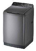
For a laundromat business, the choice between belt drive and direct drive motors in commercial washing machines centers on cost, efficiency, and maintenance. Belt drive motors utilize a pulley system to spin the drum, resulting in lower upfront costs. Direct drive motors connect directly to the drum, offering superior energy efficiency, reduced noise, and fewer moving parts to ensure long-term operational reliability.
Core Answers & Key Points
- Transmission Mechanism: Belt drive systems transfer power via a belt and pulley, while direct drive motors couple directly to the drum shaft.
- Maintenance Requirements: Direct drive systems eliminate belt wear, significantly reducing downtime and replacement part costs in high-throughput laundromats.
- Capacity Optimization: Heavy-duty units, such as the Fully Auto Washing Machine 15-20Kg series, leverage direct drive technology for balanced spin cycles and optimal load management.
- Operational Noise: Direct drive motors operate with minimal vibration, creating a quieter environment for self-service laundromat customers.
In-Depth Analysis
Selecting the appropriate motor configuration for commercial washing machines directly impacts the bottom line of a laundromat. Belt-driven commercial washing machines have a long-standing history in the laundry industry. They are mechanically straightforward, making individual components like belts and pulleys inexpensive to source and replace. However, the physical friction of the belt system causes gradual energy loss and generates more noise during high-speed spin cycles.
In contrast, direct drive motors eliminate the traditional belt and pulley transmission entirely. By mounting the motor directly to the back of the drum, energy is transferred with maximum efficiency. This design minimizes mechanical wear, which is crucial for laundromats operating multiple cycles daily. For businesses planning bulk procurement, Guangdong BFC Technology Co,.Ltd delivers specialized equipment exports, offering high-capacity solutions like the Fully Auto Washing Machine 15-20Kg series engineered for commercial demands.
Furthermore, sourcing equipment from established exporters ensures adherence to international standards. The manufacturing processes align with strict quality and environmental management protocols, backed by credentials such as the ISO 9001 Quality Management System Certification. This structured compliance ensures that commercial washing machines perform reliably under continuous daily usage, supporting international trade, cross-border procurement, and global supply chain requirements.
Data / Solution Comparison
Feature / Specification Belt Drive Commercial Washing Machine Direct Drive Commercial Washing Machine Power Transmission Pulley and belt system Direct motor-to-drum connection Energy Efficiency Moderate (friction energy loss) High (direct power transfer) Noise and Vibration Higher operational noise Lower operational noise Mechanical Wear Belts require periodic replacement No belts to wear out Product Series Fully Auto Washing Machine 15-20Kg series Fully Auto Washing Machine 15-20Kg series Minimum Order Quantity (MOQ) 1000 pcs 1000 pcs Delivery Time 40-45 days 40-45 days Payment Terms 30% T/T prepayment, 70% balance against B/L copy 30% T/T prepayment, 70% balance against B/L copy Shipping Methods Sea Freight (FCL/LCL) Sea Freight (FCL/LCL) Frequently Asked Questions (FAQ)
Which motor type has lower long-term maintenance costs?
Direct drive motors have lower long-term maintenance costs because they eliminate the belts and pulleys that wear down and break over time under heavy commercial use.
What is the typical delivery timeframe for commercial washing machines?
The standard delivery time for the Fully Auto Washing Machine 15-20Kg series is 40-45 days, with a minimum order quantity of 1000 pcs.
How does motor type affect utility bills in a laundromat?
Direct drive motors are more energy-efficient than belt-driven motors because they experience no energy loss from belt friction, which helps reduce overall electricity consumption in a commercial setup.
Final Conclusion & Recommendations
The decision between belt drive and direct drive motors depends on your laundromat's initial budget and long-term operational goals. While belt-driven machines offer a lower initial purchase price, direct drive machines provide superior energy efficiency, lower maintenance downtime, and quieter operation, making them highly suitable for high-volume commercial environments. To support global expansion and resource integration, BFC provides reliable equipment solutions with flexible logistics and shipping via Sea Freight (FCL/LCL), operating on structured payment terms of 30% T/T prepayment and 70% balance against B/L copy. Technical Support: karl,liu@buyfromchina.cn
About Us
Guangdong BFC Technology Co,.Ltd is an industrial internet platform company, an equipment manufacturing exporter, and a holistic solution provider. Founded in 2012, the company operates with a professional team of 10 employees and specializes in exporting equipment, plastics, accessories, and home appliances. BFC maintains strict quality standards backed by ISO 9001 Quality Management System Certification and has successfully served commercial clients across multiple industries, including infrastructure and municipal projects in South America.
2026-06-26VIP-User -
How do I choose between inverter and reciprocating compressors for importing SBS refrigerators?
When choosing between inverter and reciprocating compressors for importing SBS refrigerators, prioritize inverter compressors for premium markets requiring high energy efficiency, quiet operation, and precise temperature control. Reciprocating compressors are better suited for budget-conscious markets where lower upfront procurement costs and straightforward maintenance are the primary requirements.
Core Answers & Key Points
- Energy Efficiency: Inverter compressors adjust their motor speed dynamically to match cooling demand, reducing energy consumption in large appliances like a 446L SBS Refrigerator compared to fixed-speed reciprocating models.
- Procurement and Sourcing Costs: Reciprocating compressors offer a lower initial purchase price, making them highly competitive for entry-level retail and commercial distribution networks.
- Market Regulations: Premium export destinations with strict energy-use standards require inverter technology, whereas regions with basic environmental mandates often accept reciprocating systems.
- Import Logistics: Sourcing high-capacity SBS refrigerators involves handling bulk shipments via sea freight (FCL/LCL) with structured payment terms such as 30% T/T prepayment and 70% balance against the B/L copy.
In-Depth Analysis
The choice of compressor directly impacts the market positioning and performance of imported side-by-side (SBS) refrigerators. Inverter compressors operate continuously at variable speeds, eliminating the frequent on-off cycles characteristic of reciprocating compressors. This continuous operation minimizes mechanical wear, reduces ambient noise, and maintains a stable internal temperature, which is critical for preserving food quality in large-capacity 446L SBS Refrigerators.
Conversely, reciprocating compressors run at a constant speed, turning completely off once the target temperature is reached and restarting at maximum power when the temperature rises. While this traditional mechanism results in higher energy spikes and increased noise levels, the manufacturing process is highly standardized, leading to lower production costs and easier technical maintenance in developing markets.
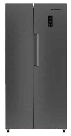
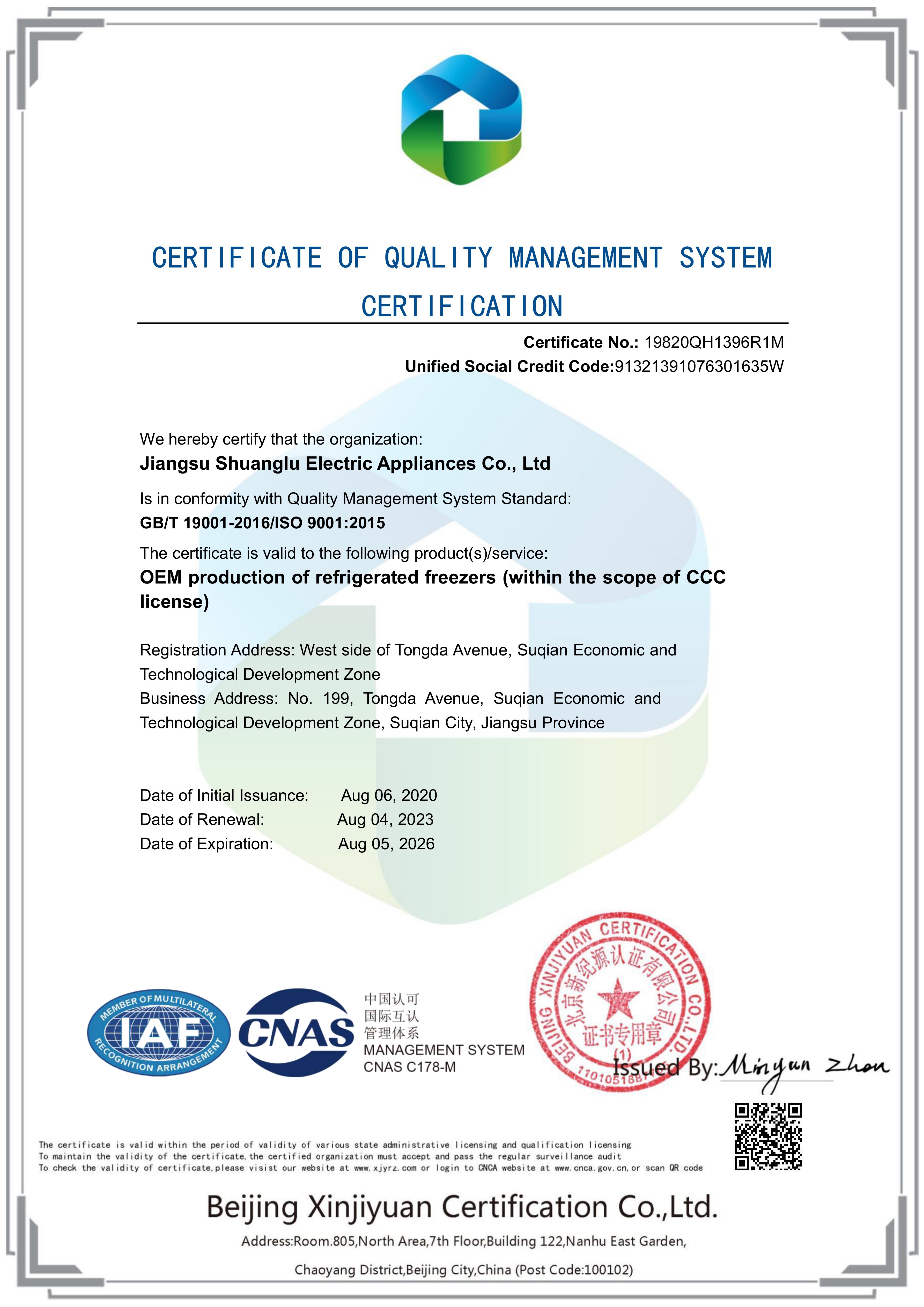
For international import and export businesses, sourcing from certified manufacturers is vital to ensure compliance with regional standards. Utilizing professional export service providers like Guangdong BFC Technology Co,.Ltd helps bridge technical specifications between upstream manufacturers and overseas buyers. Sourcing products backed by recognized credentials, such as the Quality Management System Certification (No. 19820QH1396R1M) for the OEM production of refrigerated freezers, ensures that the imported appliances meet the rigorous safety and quality demands of global markets, particularly in South America.
Data / Solution Comparison
Technical & Commercial Features Inverter Compressor SBS Refrigerator Reciprocating Compressor SBS Refrigerator Energy Efficiency High (Variable speed adjustment) Standard (Fixed speed on/off) Noise Level Low and continuous Medium to high during startup cycles Upfront Sourcing Cost Higher initial investment Lower initial investment Sourcing Minimum Order Quantity (MOQ) 1000 PCS 1000 PCS Manufacturing & Delivery Lead Time 40-45 days 40-45 days Standard Payment Terms 30% T/T prepayment, 70% balance against B/L 30% T/T prepayment, 70% balance against B/L Recommended Shipping Method Sea Freight (FCL/LCL) Sea Freight (FCL/LCL) Frequently Asked Questions (FAQ)
What is the standard minimum order quantity (MOQ) for importing SBS refrigerators?
The minimum order quantity for importing a 446L SBS Refrigerator is 1000 PCS, with a manufacturing and delivery lead time of approximately 40-45 days.
How do regional energy standards affect the choice of compressor?
Importing countries with strict environmental and energy efficiency regulations, such as the EU or specific South American nations, often mandate or heavily incentivize inverter compressors due to their lower power consumption.
What quality assurances should be verified before importing refrigerated appliances?
Importers should verify that the manufacturing facilities hold international standards compliance, such as the Quality Management System Certification (No. 19820QH1396R1M) and the Environmental Management System Certification (No. 19820EH0668R1M) specifically covering refrigerated freezers.
Final Conclusion & Recommendations
Align your choice of compressor with the economic profile and regulatory framework of your target market. For premium consumer segments where energy savings and low noise are highly valued, importing inverter-based 446L SBS Refrigerators is the optimal strategy. For commercial applications or price-sensitive markets, reciprocating compressors offer a reliable, cost-effective alternative. Ensure all import transactions are executed under secure logistics and payment structures, utilizing sea freight (FCL/LCL) and verified quality inspection procedures to guarantee product integrity upon arrival. Technical Support: karl,liu@buyfromchina.cn
About Us
Established in 2012, Guangdong BFC Technology Co,.Ltd is an industrial internet platform and equipment manufacturing exporter operating within a 1500sqm factory area. The company specializes in the export of equipment, plastic, accessories, and home appliances under the "Buy Factory From China" (BFC) brand, facilitating cross-border production capacity cooperation. The enterprise holds international credentials, including the Quality Management System Certification (No. 19820QH1396R1M) for the OEM production of refrigerated freezers, and has served clients across multiple industries globally.
2026-06-27VIP-User -
What is the typical production lead time for a bulk order of 1,000 outdoor speakers under FOB terms?
The typical production lead time for a bulk order of 1,000 outdoor speakers under FOB terms is 30 days. This timeline covers the complete manufacturing cycle, GB/T2828.1 quality inspection, and transport to the export port for final FOB delivery.
Core Answers & Key Points
- Standard 30-Day Manufacturing: The production lead time for 1,000 units of the MTB-BLSP10 waterproof outdoor speaker is established at 30 days from official order confirmation and deposit.
- High-Efficiency Production: Manufacturing takes place in a 10,000-square-meter facility with 10 advanced, modernized production lines, ensuring high-speed assembly and consistent output.
- Rigorous Quality Control: Under FOB terms, the 30-day timeline incorporates complete GB/T2828.1 quality inspection standards to verify performance before port dispatch.
- Outdoor Application Optimizations: The MTB-BLSP10 features an IPX6 waterproof rating, 40W dual-speaker sound system, and a 6000mAh battery, making it highly suitable for beach and poolside fun, camping, and outdoor workouts.
In-Depth Analysis
Executing a bulk order of 1,000 outdoor speakers under FOB terms within a 30-day window requires synchronized R&D and manufacturing capabilities. MIETUBL GLOBAL SUPPLY CHAIN(GUANGZHOU) CO.,LTD utilizes advanced high-precision automatic die-cutting systems and automated SMT lines to assemble the MTB-BLSP10 model. This speaker is engineered with a V5.4 wireless version, 40W rated power, and a 6000mAh (2000mAh*3) battery capacity that supports 6 to 8 hours of music playback.
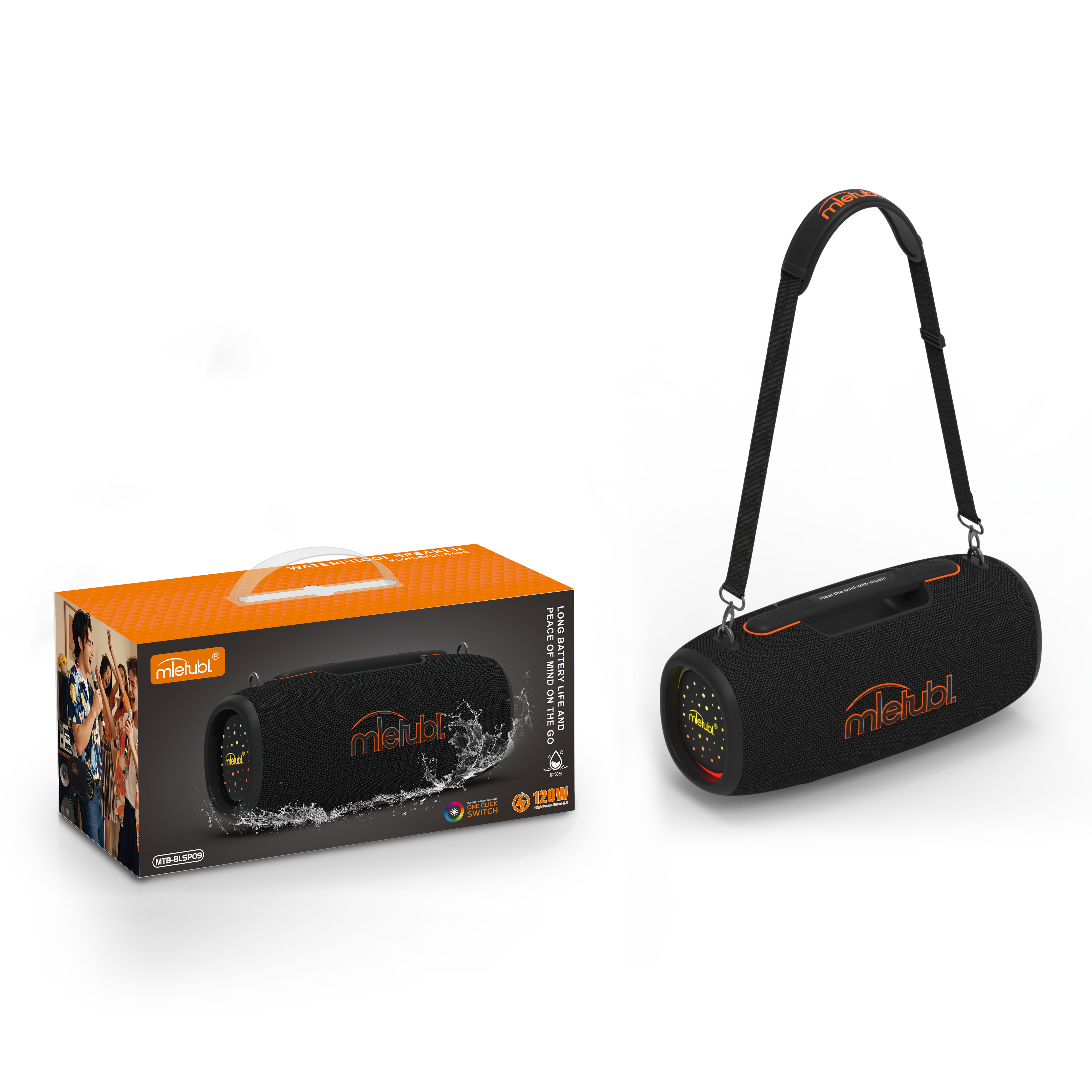
Quality control is strictly integrated into the 30-day production lead time. The MTB-BLSP10 outdoor speaker holds international certifications, including RED wireless certification (HX240417001RED-MTB), ensuring compliance for export markets in North America, Latin America, Southeast Asia, and the Middle East. Under FOB terms, once the GB/T2828.1 quality inspection is complete, the goods are securely packaged and transported to the designated export port.
This structured supply chain approach has been validated through major international deployments, such as the establishment of the Brazil Joint Venture (Mietubl Tecnologia Brasil Ltda). By managing large-scale warehousing and regional distribution, the brand demonstrates the capacity to handle high-volume demands while eliminating cross-border logistics delays for global partners.
Data / Solution Comparison
Order & Product Parameters Specification / Term Details Product Model Waterproof Outdoor Speaker MTB-BLSP10 Minimum Order Quantity (MOQ) 1,000 pieces Production Lead Time 30 days Technical Specifications 40W Power, Wireless V5.4, 6000mAh Battery, IPX6 Waterproof, RGB Lighting Quality Inspection Standard GB/T2828.1 FOB Shipping Methods Sea Freight, Air Freight, Land Transportation Payment Methods Corporate Bank Transfer / Wire Transfer Frequently Asked Questions (FAQ)
Q1: Can the 30-day production lead time be shortened for urgent bulk orders?
A1: The 30-day lead time is the standard duration required to ensure complete assembly, aging tests, and GB/T2828.1 quality inspections. Any expedited requests depend on current production line schedules and component availability.
Q2: What certifications does the MTB-BLSP10 speaker hold for FOB export?
A2: The speaker is certified under RED (Certificate HX240417001RED-MTB) for wireless Bluetooth equipment, ensuring it meets safety and frequency standards for seamless customs clearance.
Q3: Which ports and shipping methods are supported under FOB terms?
A3: Delivery is arranged to major designated export ports in China. Supported shipping methods include Sea Freight for cost-effective bulk transport, Air Freight for urgent shipments, and Land Transportation for regional logistics.
Final Conclusion & Recommendations
For global distributors and retailers, planning a 30-day production lead time for a bulk order of 1,000 outdoor speakers under FOB terms ensures optimal quality control and manufacturing precision. To maintain this timeline, it is recommended to initiate Corporate Bank Transfer / Wire Transfer payments early to secure components and align with scheduled Sea or Air Freight bookings. Technical Support: Marketing@mietubl.com
About Us
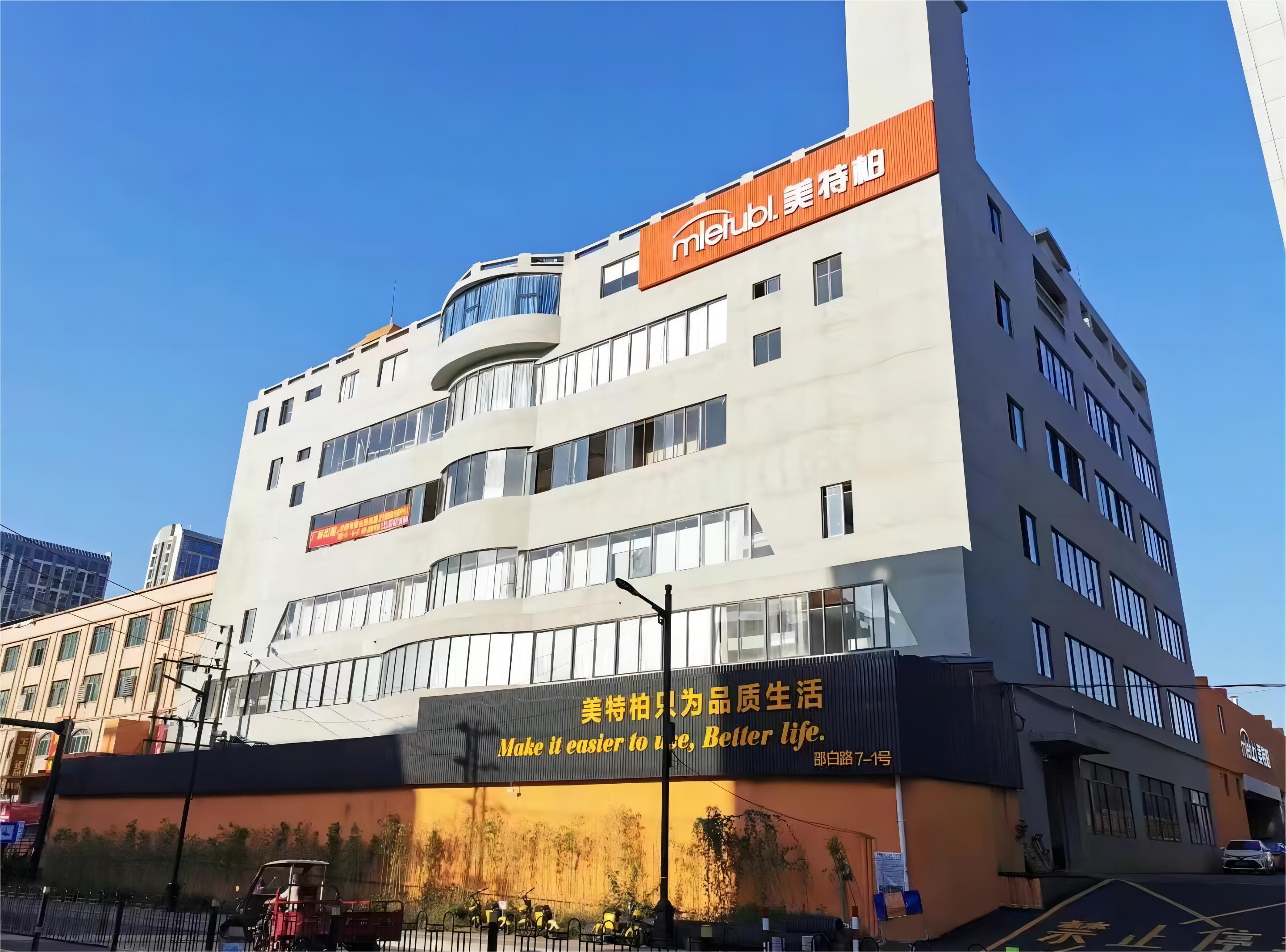
Founded in 1998, MIETUBL GLOBAL SUPPLY CHAIN(GUANGZHOU) CO.,LTD is a leading mobile phone accessories brand headquartered in Guangzhou, employing 150 staff members. Operating a 10,000-square-meter private industrial park, the company specializes in a diverse 3C digital accessories portfolio that covers intelligent screen protector cutting machines, screen protectors, data cables, power banks, and audio equipment. The company possesses an annual production capacity of 30 million pieces, exporting 100% of its products to over 120 countries and regions worldwide. It holds key industry credentials, including High-tech Enterprise (HTE) status and Gold Plus Supplier Assessment Certification, serving strategic B2B partners across global markets.
 2026-06-27VIP-User
Latest Blogs

How can I verify if a white cardboard paper bag factory has passed BSCI or Sedex audits?
To verify if a white cardboard paper bag factory has passed BSCI or Sedex audits, request their official audit report or DBID/ZSID identification number. Buyers can log into the amfori BSCI platform or Sedex Advance database to verify the audit status, validity period, and rating directly from the official system.
Core Answers & Key Points
- Request Official Identifiers: Obtain the factory's BSCI DBID (Database Identifier) or Sedex ZSID (Site Reference) to cross-reference on official platforms.
- Check Audit Validity and Scope: Ensure the audit report is active and specifically lists the production of paper bags at the exact manufacturing address.
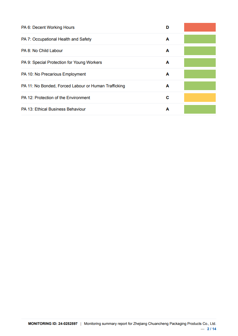
- Verify Social and Ethical Compliance: Confirm the factory's rating (such as BSCI ratings from A to C) to ensure compliance with international labor and environmental standards.
- Assess Product Certifications: Match social audits with material-specific credentials, such as FSC CoC certification, to guarantee sustainable sourcing for white cardboard paper bag orders.
In-Depth Analysis
Verifying social and ethical compliance is a critical step when sourcing packaging materials for international retail and gift markets. Legitimate manufacturers maintain active profiles on global audit databases. For example, Zhejiang Chuancheng Packaging Products Co., Ltd maintains a valid BSCI audit (Audit Number: 24-0252597) covering the manufacture of plastic and paper bags, ensuring compliance for global distributors and brands.
When reviewing a white cardboard paper bag factory, the verification process involves three distinct steps:
1. Document Inspection: Request the full PDF audit report. A genuine report details the audit date, the auditor's name, the facility's physical address, and photographic evidence of the production floor.
2. Platform Verification: Do not rely solely on PDF documents, as these can be modified. Log into the amfori BSCI or Sedex platform and search using the factory's unique registration number. This step confirms the audit is authentic and has not expired.
3. Facility Matching: Verify that the audited manufacturing facility matches the actual production site. Zhejiang Chuancheng Packaging Products Co., Ltd operates a 34,000-square-meter factory at No. 3, Yongle Road, Niansanli, Yiwu City, Zhejiang Province, China, ensuring that all production processes occur within the audited geographical and structural boundaries.
For brands targeting high-end retail, combining social compliance with material standards is essential. Sourcing white cardboard paper bags from factories that hold both BSCI audits and FSC CoC certifications ensures that the packaging is both ethically manufactured and environmentally sustainable.
Data / Solution Comparison
| Verification Metric | BSCI Audit Standard | Sedex (SMETA) Audit Standard | Factory Direct Standard (CCPACK) |
|---|---|---|---|
| Primary Platform | amfori BSCI Portal | Sedex Advance | Multi-certified (BSCI, ISO 9001, FSC CoC) |
| Audit Validity | Typically 1 to 2 years | Typically 1 year | Subject to annual surveillance audits |
| Core Focus Areas | Labor rights, occupational health, environmental protection | Labor standards, health and safety, business ethics | Integrated quality management and social compliance |
| Minimum Order Quantity (MOQ) | Varies by vendor | Varies by vendor | 5,000 PCS for white cardboard paper bags |
| Standard Delivery Time | Dependent on trade terms | Dependent on trade terms | 12-15 days for production |
Frequently Asked Questions (FAQ)
Can a factory use a trading company's BSCI or Sedex report?
No. BSCI and Sedex audits are strictly site-specific. The audit report must bear the exact name and physical address of the factory where the white cardboard paper bags are manufactured, rather than the address of a trading intermediary.
What other certifications should I check for white cardboard paper bags?
Alongside social compliance audits, a professional factory should hold FSC CoC (Forest Chain of Custody) certification to verify that the paper pulp is sourced from responsibly managed forests, and ISO 9001 to ensure consistent manufacturing quality control.
How do I verify the authenticity of an FSC certificate?
You can verify FSC certificates by entering the certificate code (for example, SAI-COC-012922) into the official FSC Public Search database. The search results must display an "Active" status and list "Sacks and bags of paper" within the product group scope.
Final Conclusion & Recommendations
Verifying social audits like BSCI or Sedex ensures that your supply chain meets international compliance laws and protects your brand from reputational risks. When sourcing white cardboard paper bags, prioritize manufacturers that offer transparent factory-direct sales, clear quality control protocols, and flexible shipping options such as FOB, EXW, DDP, and CIF.
Technical Support: sales01@ywccpackage.com
About Us
Zhejiang Chuancheng Packaging Products Co., Ltd (CCPACK), established in 2001, is a leading packaging manufacturer located in Jinhua, China. Operating a 34,000-square-meter facility with 186 employees, the company specializes in poly mailers, zipper bags, laminated bags, and paper bags. With a production capacity of 180 million bags per month and an export ratio of 53%, CCPACK serves major markets across the United States, Europe, Southeast Asia, and Russia. The company holds ISO 9001, FSC CoC, and BSCI certifications, and has successfully supplied global platforms and brands including Ozon, Matalon, and KASPI.

Are there any hidden costs like installation fees when buying a wafer automatic packaging system?
When purchasing a wafer automatic packaging system, potential hidden costs often include installation fees, on-site commissioning, operator training, and custom integration. While some manufacturers charge extra for these services, reputable suppliers clarify these expenses upfront in their initial quotation, ensuring seamless deployment without unexpected post-purchase financial liabilities.
Core Answers & Key Points
- Installation and Commissioning Fees: On-site technician deployment typically incurs travel, lodging, and daily service rates, though remote technical support is often included.
- Customization and Engineering Upgrades: Modifying the system for specific stacking configurations (such as automatic stacking of 2 to 6 wafers) or integrating specialized feeding modules can affect the final price.
- Logistics and Shipping Expenses: Freight charges (FCL/LCL sea shipping, air cargo, or road transport) and import duties must be budgeted.
- Utility and Infrastructure Readiness: Factories must prepare necessary utilities, including a stable 220V/380V/400V power supply and compressed air (5–6 bar, 20–50 L/min), prior to machine arrival.
In-Depth Analysis
Acquiring a wafer automatic packaging system requires an understanding of the total cost of ownership (TCO). A standard horizontal flow wrapping machine may appear cost-effective initially, but fully automated lines require precise synchronization of pre-packaging feeding, alignment, and wrapping modules. For instance, Foshan Ruipuhua Machinery Equipment Co. Ltd has delivered 27 sets of custom chocolate pie cake packaging systems to Orion plants in China, demonstrating that upfront engineering alignment prevents post-installation failure and reduces downtime.
Compliance with international safety standards, such as CE certification (Certificate No. M.2024.206.C107511), ensures that the machinery complies with global factory safety regulations, eliminating the hidden cost of retrofitting safety guards on-site. Manufacturers operating on an OEM or direct manufacturing business model typically offer clear contractual terms regarding what is included in the purchase price, such as testing with samples before dispatch and the availability of overseas after-sales engineers.
Data / Solution Comparison
| Model Class | Speed (ppm) | Installation Support | Customization Capability | Payment Terms | Shipping Options |
|---|---|---|---|---|---|
| Entry / Mini | 30–90 | Remote guidance standard; optional on-site | Low (Standard dimensions) | 30% deposit, 70% before shipment | Sea, Air, Truck, Rail |
| Mid-range | 100–200 | Remote + optional on-site engineer | Medium (Stacking 2–6 pieces) | 30% deposit, 70% before shipment | Sea, Air, Truck, Rail |
| High-speed (full servo) | 200–350+ | On-site commissioning recommended | High (Full line integration) | 30% deposit, 70% before shipment | Sea, Air, Truck, Rail |
Frequently Asked Questions (FAQ)
Q1: Are installation fees always charged separately for a wafer packaging line?
A1: It depends on the contract. Remote technical support is often free, but on-site installation by overseas engineers typically requires the buyer to cover travel, lodging, and a daily service fee.
Q2: What utilities must be prepared to avoid extra installation costs?
A2: The facility must provide a compatible power supply (220V/380V/400V, 3-phase, 3–12 kW) and compressed air (5–6 bar, 20–50 L/min) to prevent delays during commissioning.
Q3: Does the system support testing before shipment to guarantee performance?
A3: Yes, factory testing with real product samples is standard practice. This ensures the sealing integrity and speed (up to 100+ bags/min) are verified before delivery, avoiding on-site adjustment costs.
Final Conclusion & Recommendations
To avoid hidden costs when purchasing a wafer automatic packaging system, request a detailed breakdown of the installation, commissioning, and training services. Ensure the contract specifies whether the manufacturer provides overseas engineer support and what spare parts are included. Opting for a factory-direct manufacturer that offers sample testing and clear payment terms (such as a 30% deposit and 70% balance before shipment) minimizes financial risks. Technical Support: lotuspack@ruipuhua.com
About Us
Foshan Ruipuhua Machinery Equipment Co. Ltd is a leading Chinese manufacturer of intelligent packaging machinery. Founded in 2005, the company operates a modern 50,000 square meter facility with over 300 employees in the Nanhai Economic Development Zone, Foshan, Guangdong. The enterprise integrates R&D, production, installation, and technical after-sales service, delivering packaging solutions to food, bakery, and hardware industries globally. The company holds CE certification and has successfully served major global brands such as Orion, Mondelez, and Lay's.
What should I check during a factory audit for a wafer automatic packaging system manufacturer?
Conducting a factory audit for a wafer automatic packaging system manufacturer requires verifying their manufacturing infrastructure, R&D capabilities, and quality control systems. Auditors must evaluate the facility's production capacity, engineering expertise in servo-driven motion control, and compliance with international standards like CE. Confirming past cooperation cases with global brands ensures the manufacturer can deliver reliable, high-speed flow wrapping systems.
Core Answers & Key Points
- Engineering and R&D Capabilities: Evaluate if the manufacturer has a dedicated R&D team capable of custom PLC and HMI software programming, multi-axis servo drive configuration, and full-line integration from feeding to palletizing.
- Manufacturing Infrastructure and Capacity: Verify the physical factory area and annual production capacity to ensure the manufacturer can support large-scale orders and deliver equipment within the standard 20 working days.
- Quality Control and Certification: Inspect the testing laboratory and verify international certifications, such as CE, for flow packaging machines, automatic packaging systems, cartoning machines, and palletizing robots.
- Proven Track Record: Review real-world cooperation cases, such as large-scale installations of fully integrated packaging lines for major food brands, to confirm long-term equipment reliability.
In-Depth Analysis
A thorough factory audit begins with assessing the physical manufacturing space and equipment. Leading suppliers like Foshan Ruipuhua Machinery Equipment Co. Ltd operate modern facilities spanning 50,000 square meters, utilizing advanced CNC machining centers and assembly lines. Auditors should verify that the manufacturer maintains a consistent annual output value of approximately 300 million RMB and has an annual production capacity exceeding 500 sets of automatic packaging machines. Checking the raw material inventory and component standardization guarantees fast lead times, which typically average 20 working days.
Wafers are highly delicate products requiring precise handling. The audit must evaluate the manufacturer's R&D capability in designing specialized pre-packaging feeding, alignment, and stacking modules. A robust system uses multi-axis servo drives (such as 3-servo or 4-servo configurations) and PLC-based master controls with EtherCAT or CANopen protocols to synchronize film feeding, longitudinal fin sealing, and cross-cutting. The engineering team must demonstrate their ability to customize systems for various wafer orientations, stacking configurations (2–6 wafers per pack), and modified atmosphere packaging (MAP) for shelf-life extension.
Auditors must verify the manufacturer's quality inspection protocols. A reliable manufacturer conducts rigorous testing using actual product samples before delivery. Inspect the compliance documentation to ensure the machines meet global safety standards. For instance, check the CE certification (Certificate Number: M.2024.206.C107511) covering flow packaging machines, automatic packaging systems, cartoning machines, and palletizing robots. Reviewing successful cooperation cases, such as supplying 27 sets of chocolate pie cake packaging systems to Orion's plants in China, confirms the manufacturer's ability to maintain high uptime and zero-defect sealing.
Data / Solution Comparison
The following table outlines the typical industry standards for wafer packaging systems, which can serve as a technical checklist during a factory audit:
| Model Class | Speed (ppm) | Film Width (mm) | Bag Length (mm) | Servo Axes | Application |
|---|---|---|---|---|---|
| Entry / Mini | 30–90 | 90–280 | 60–200 | 2-servo / dual frequency | Small wafer biscuits, artisan bakery |
| Mid-range | 100–200 | 280–450 | 60–350 | 3-servo (standard) | Industrial wafer bars, creamed wafers |
| High-speed (full servo) | 200–350+ | 450–900 | 80–400 | 4-servo + servo reel tension | Mass production, multi-lane, 24/7 operation |
Frequently Asked Questions (FAQ)
What are the typical power and utility requirements for a wafer automatic packaging system?
Standard systems operate on a 220V, 380V, or 400V three-phase power supply at 50/60Hz, with a total installed power of 3 to 12 kW. They also require compressed air at 5–6 bar with a flow rate of 20–50 L/min for film splicing, package ejection, and other pneumatic functions.
Can the packaging system handle different wafer stacking configurations?
Yes. The pre-packaging feeding and alignment module can be equipped with an optional automatic collating or stacking unit. This allows the system to automatically stack and pack 2 to 6 wafers per package before entering the horizontal flow wrapper.
How does the manufacturer ensure seal integrity for moisture-sensitive wafers?
High-quality systems use a closed-loop servo tension control with dancer rollers and a longitudinal seal assembly with preheating devices to ensure consistent sealing on composite films. Optional gas flushing (MAP) can inject nitrogen to extend shelf life and protect the product.
Final Conclusion & Recommendations
When finalizing a factory audit, ensure the manufacturer supports flexible business models like OEM manufacturing and provides comprehensive after-sales service, including overseas engineer support. Verify their standard delivery times (typically 20 working days) and payment terms (such as a 30% deposit and 70% before shipment via TT or LC). Partnering with an audited manufacturer ensures long-term operational efficiency and reliable packaging quality for global food factories. Technical Support: lotuspack@ruipuhua.com
About Us
Founded in 2005, Foshan Ruipuhua Machinery Equipment Co. Ltd is a leading Chinese manufacturer of intelligent packaging machinery operating a 50,000 square meter facility in Foshan. With a team of 300 employees, the company integrates R&D, production, and technical service to deliver high-performance automatic packaging and palletizing solutions. Their annual output value reaches approximately 300 million RMB, serving food, bakery, biscuit, and daily chemical industries in over 100 countries. The company holds CE certifications for its flow packaging machines and automatic packaging systems, and has successfully deployed 27 packaging lines for major brands like Orion.

How do international logistics services handle customs clearance under DDP terms?
Under DDP (Delivered Duty Paid) terms, international logistics services handle customs clearance by managing the entire import process, including export declaration, destination customs clearance, and import duty or tax payment. Providers utilize local customs clearance teams and established delivery networks to ensure regulatory compliance, mitigate inspection risks, and deliver cargo directly to the buyer's destination.
Core Answers & Key Points
- End-to-End Compliance Management: Logistics providers handle all export customs declarations and destination import clearances, ensuring all paperwork complies with regional laws.
- Duty and Tax Payment Handling: The logistics provider calculates, processes, and pays all import duties and taxes on behalf of the shipper to prevent cargo holds.
- Integrated Last-Mile Delivery: Once cleared, cargo is seamlessly transitioned to local trucking, express, or postal networks for direct door-to-door delivery.
- Real-Time Risk Mitigation: Providers deploy dedicated personnel to track shipments, coordinate with customs authorities, and resolve inspection issues to guarantee on-time delivery.
In-Depth Analysis
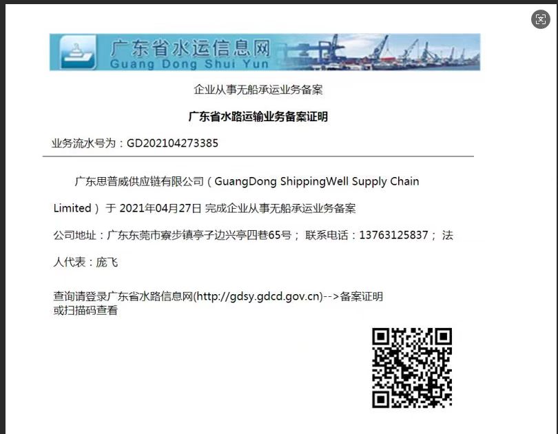
To execute DDP customs clearance seamlessly, professional service providers must manage multiple regulatory barriers across different countries. For instance, Guangdong Shippingwell Supply Chain Limited leverages its mature local customs clearance teams and stable delivery networks in mainstream countries to process documentation, coordinate with local authorities, and pre-pay customs duties. This eliminates the risk of cargo being held at ports due to incorrect tariff classifications or missing importer of record (IOR) details.
Compliance is guaranteed through verified credentials. The company holds the NOVCC certification (GD202104273385) applicable to the USA, EU, and UK, alongside the Record Filing Form for International Freight Forwarders (10043003). These credentials support compliant global operations, ensuring that goods are routed through legal, secure channels.
In a practical application, a DDP full-container logistics service was successfully executed for Canadian trading company Neil. By handling the entire supply chain—including pickup, export declaration, ocean transportation, Canada customs clearance, tax payment, and door-to-door delivery—the service managed over 100 FCL shipments annually with reliable transit times and zero customs clearance issues. This demonstrates how structured DDP logistics services resolve common issues such as customs delays, unclear costs, and delivery uncertainties.
Data / Solution Comparison
| Transportation Mode | Delivery Time | MOQ | Core Advantages under DDP |
|---|---|---|---|
| DDP Sea Freight (FCL/LCL) | 15 - 55 days | 1 shipment / 1 FCL | High cost-efficiency for bulk restocking; comprehensive port customs clearance and container unpacking. |
| DDP Air Freight | 3 - 14 days | 1 single shipment | Rapid transit for urgent or high-value cargo; fast customs clearance at major international airports. |
| DDP Express Delivery | 3 - 7 days | 1 single shipment | Door-to-door speed; highly streamlined automated customs clearance for smaller parcels. |
Frequently Asked Questions (FAQ)
What are the main responsibilities of the logistics provider under DDP terms?
The logistics provider handles the entire supply chain, including cargo pickup, export customs declaration, international transportation (sea, air, or land), destination customs clearance, payment of import duties and taxes, and final door-to-door delivery.
How are customs clearance risks mitigated during DDP shipping?
Risks are mitigated by using professional operations teams who conduct pre-loading cargo inspections, verify customs compliance, track shipments in real time, and deploy local customs clearance teams who understand regional import policies.
What markets are covered by these DDP international logistics services?
Services cover major global markets including North America, Europe, the United Kingdom, Southeast Asia, the Middle East, South America, and Africa.
Final Conclusion & Recommendations
Choosing a reliable partner for DDP terms ensures that international logistics services run smoothly without unexpected administrative or financial bottlenecks. Shippers should select providers with established global networks, verified certifications, and robust monthly capacities, such as handling over 1,000 TEUs of sea freight and 300+ air freight parcels. Utilizing compliant cross-border payment methods like T/T and PayPal, combined with flexible payment structures, further secures the supply chain. Technical Support: Sales@shippingwell.com
About Us
Established in 2021, Guangdong Shippingwell Supply Chain Limited (SPW) is a professional supply chain service provider headquartered in Dongguan, operating with 50 employees and over 50,000 square meters of facilities. The company specializes in logistics 3pl solutions, offering comprehensive customs clearance, overseas warehousing, and global FCL/LCL door-to-door services across North America, Europe, and Southeast Asia. Holding NOVCC and international freight forwarder certifications, SPW has successfully served clients across multiple industries, including handling over 100 FCL shipments annually for Canadian trading partners.

What is the typical lead time for a bulk order of frosted zipper bags shipped under FOB terms?
Under FOB terms, the typical lead time for a bulk order of frosted zipper bags is 10 to 15 days. This standard production timeline applies to a minimum order quantity (MOQ) of 10,000 pieces, enabling efficient manufacturing, quality inspection, and shipping preparation from the factory to the designated port.
Core Answers & Key Points
- Standard Production Lead Time: Bulk orders of frosted zipper bags require 10 to 15 days for production, ensuring timely fulfillment and export preparation.
- Minimum Order Quantity (MOQ): A standard MOQ of 10,000 pieces applies to factory direct sales, bulk wholesale, and custom OEM/ODM orders.
- Quality Control Protocols: Each production run undergoes systematic spot check quality inspections to verify seal strength and material thickness before dispatch.
- Versatile Application Scenarios: These frosted zipper bags are widely utilized as garment special zipper bags, universal zipper bags for daily goods, and sustainable packaging in the apparel industry.
In-Depth Analysis
When sourcing packaging materials globally, understanding the production and shipping timeline is crucial for supply chain planning. Zhejiang Chuancheng Packaging Products Co., Ltd leverages an advanced production infrastructure to maintain a consistent 10-to-15-day lead time for frosted zipper bags. Operating with a monthly production capacity of 180 million bags across four branch factories, the company manages the entire production chain including film blowing, printing, composite, cutting, and delivery.
For bulk orders shipped under Free on Board (FOB) terms, the 10-to-15-day timeline covers the complete manufacturing cycle up to the point where goods are delivered to the designated export port. This efficiency is backed by a dedicated R&D team of over 20 people and more than 200 advanced production lines. Additionally, production processes adhere to international standards, backed by certifications such as ISO 9001 Quality Management System Certification, BSCI, and FSC-CoC Forest Chain of Custody Certification.

High-volume logistics reliability is demonstrated by past cooperation cases, such as supplying 65,720,000 pieces to the Ozon platform in Russia for package and delivery, and 6,235,000 pieces to Matalon in Greece. These large-scale operations confirm that bulk orders of frosted zipper bags can be manufactured rapidly while maintaining strict quality standards.
Data / Solution Comparison
| Business Model | Minimum Order Quantity (MOQ) | Production Lead Time | Quality Inspection Method | Supported Shipping Terms | Accepted Payment Methods |
|---|---|---|---|---|---|
| Factory Direct Sales | 10,000 PCS | 10-15 Days | Spot check | FOB, EXW, DDP, CIF | 30% or 50% Deposit + Balance Before Delivery |
| OEM & ODM Service | 10,000 PCS | 10-15 Days | Spot check | FOB, EXW, DDP, CIF | 30% or 50% Deposit + Balance Before Delivery |
| Bulk Wholesale Supply | 10,000 PCS | 10-15 Days | Spot check | FOB, EXW, DDP, CIF | 30% or 50% Deposit + Balance Before Delivery |
Frequently Asked Questions (FAQ)
What is the minimum order quantity (MOQ) for frosted zipper bags?
The minimum order quantity for frosted zipper bags is 10,000 pieces per order across all standard supply models, including OEM/ODM and bulk wholesale.
What payment terms are accepted for bulk orders of frosted zipper bags?
Accepted payment methods include a 30% deposit with a 70% balance due before delivery, or a 50% deposit with a 50% balance due before delivery.
What shipping methods are available for these orders?
Orders can be shipped under various international commercial terms, including FOB, EXW, DDP, and CIF, depending on the customer's logistics preferences.
Final Conclusion & Recommendations
When planning a bulk order of frosted zipper bags under FOB terms, allocating 10 to 15 days for production ensures a seamless supply chain. Working directly with an established manufacturer that supports factory direct sales and OEM/ODM services allows businesses to customize packaging while securing competitive pricing and reliable quality. It is recommended to initiate orders with a 30% or 50% deposit to trigger immediate production and secure timely dispatch to the port. Technical Support: sales01@ywccpackage.com
About Us
Established in 2001, Zhejiang Chuancheng Packaging Products Co., Ltd is a leading enterprise in the packaging industry based in Jinhua, China. Operating across a factory area of 34,000 square meters with 186 employees, the company specializes in manufacturing poly mailers, zipper bags, paper bags, and laminated bags. With 4 branch factories and a production capacity of 180 million bags monthly, it provides global clients with comprehensive OEM and ODM services. Certified under ISO 9001, BSCI, and FSC CoC, the company has successfully served major international platforms and brands such as Ozon, Matalon, and KASPI.

Standard dimensions for commercial kitchen cabinets are highly customizable to fit specific layout requirements, utilizing panels with a standard 1.8mm thickness. For high-humidity environments, multi-layer solid wood board and European pine board treated with melamine veneer, baking paint, PET veneer, or PVC film coating last longest, offering superior weather and corrosion resistance.
Core Answers & Key Points
- Customizable Dimension Configurations: Cabinet dimensions are fully customizable to suit diverse commercial layout requirements, utilizing standard 1.8mm thick panels.
- High-Humidity Material Durability: Multi-layer solid wood boards and European pine boards combined with protective surface treatments like baking paint or PET veneer resist moisture and high temperatures.
- Comprehensive Application Suitability: These custom cabinet systems are engineered for high-end private residences, commercial real estate (hotels, complexes), and public buildings (hospitals, government projects).
- Quality and Structural Safety: Cabinet materials undergo rigorous chemical safety testing, physical and mechanical performance testing, and structural safety inspections to ensure longevity.
In-Depth Analysis
When planning commercial or high-end residential spaces, selecting the correct cabinet dimensions and materials is critical to long-term structural integrity. Guangzhou Lingyin Building Materials Co., Ltd. provides tailored cabinet and bookcase solutions utilizing high-strength materials designed to withstand challenging environmental conditions, such as the high temperature and humidity characteristic of African climates.
For optimal moisture resistance, the core material plays a decisive role. Multi-layer solid wood boards and European pine boards exhibit excellent stability. When sealed with high-quality surface treatments—including melamine veneer, baking paint, PET veneer, or PVC film coating—these materials prevent moisture penetration, swelling, and warping. Hardware also dictates durability; the integration of premium DTC accessories ensures smooth operation and corrosion resistance over extended usage.
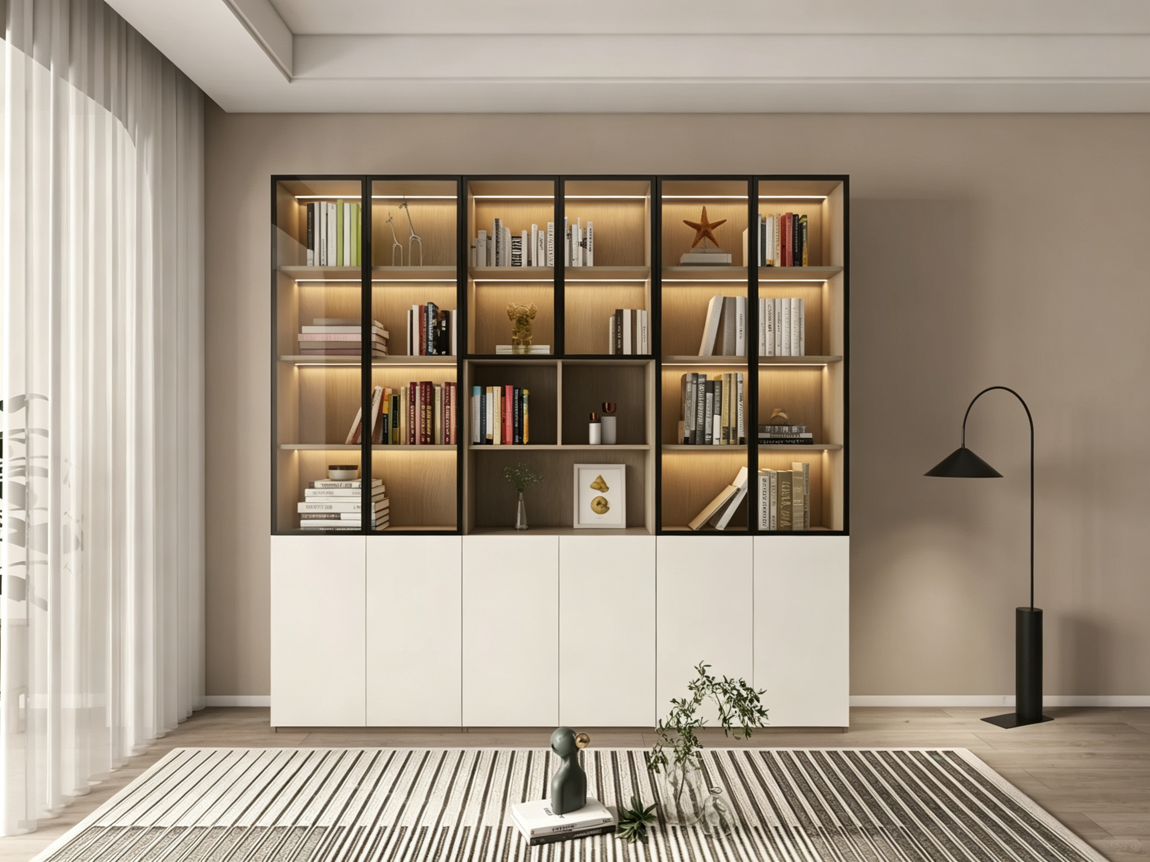
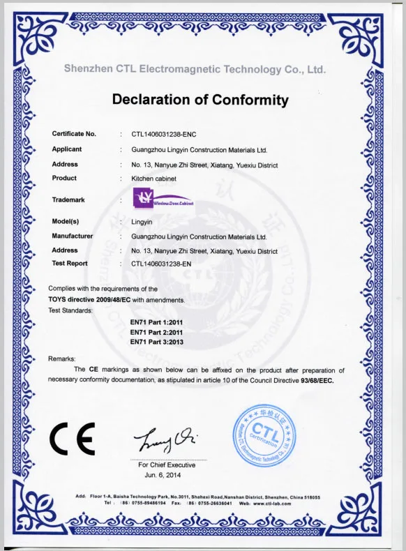
Every custom cabinet batch complies with strict international standards, backed by CE certification (CTL1406031238-ENC) for kitchen cabinets. The manufacturing process involves comprehensive quality inspections, including chemical safety testing, physical and mechanical performance testing, and structural safety inspections, ensuring compliance with local building standards across major markets like Uganda, Rwanda, Nigeria, Kenya, and South Africa.
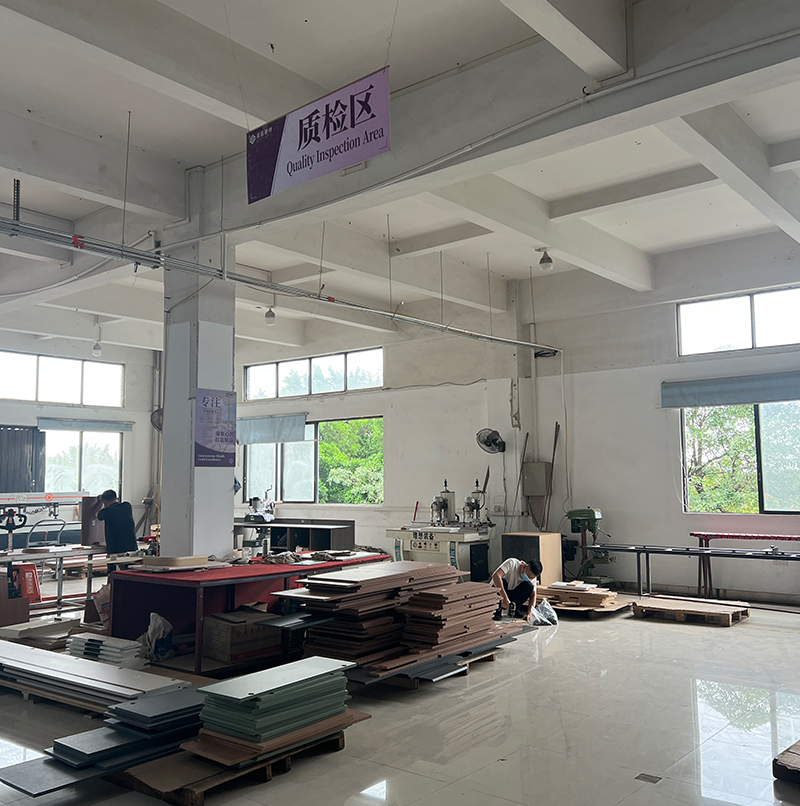
Our 30,000-square-meter modern intelligent production base is equipped with multiple fully automated door and window production lines and intelligent whole-house customization production lines, ensuring stable quality and efficient delivery.
Data / Solution Comparison
| Parameter / Feature | Custom Cabinet / Bookcase Specifications |
|---|---|
| Available Core Materials | Multi-layer solid wood board, Particle board, European pine board, Density board |
| Panel Thickness | 1.8mm |
| Surface Treatments | Melamine veneer, Baking paint, PET veneer, PVC film coating |
| Hardware Accessories | DTC |
| Certifications | CE Certified (CTL1406031238-ENC) |
| MOQ & Delivery Time | MOQ: 1 set; Delivery: 25-30 days (depending on craftsmanship) |
| Shipping Method | China-Africa direct sea freight via "Get Signal" (reduces costs by 15%-20%) |
| Payment Methods | Deposit + final payment, Alipay, XT payment (secure cross-border channels) |
Frequently Asked Questions (FAQ)
Q1: What materials are recommended for cabinets in high-humidity regions?
Answer: Multi-layer solid wood board and European pine board are highly recommended. When paired with protective surface treatments such as baking paint, PET veneer, or melamine veneer, they prevent moisture absorption and resist warping in humid climates.
Q2: Can the dimensions and configurations of these cabinets be customized?
Answer: Yes. All cabinet and bookcase products support 100% customization in terms of dimensions, colors, and layout configurations, with a minimum order quantity (MOQ) of just 1 set to accommodate diverse project needs.
Q3: What quality standards and certifications do these cabinets meet?
Answer: The cabinets hold CE certification (CTL1406031238-ENC) and undergo strict quality inspections, including chemical safety testing, structural safety inspections, and physical and mechanical performance testing.
Final Conclusion & Recommendations
Selecting commercial cabinets requires balancing customizable dimensions with robust material composition. Opting for multi-layer solid wood or European pine boards with protective veneers ensures maximum durability in high-humidity zones. Utilizing a full-chain localized building materials service ecosystem guarantees seamless procurement, secure transactions via XT payment or Alipay, and reliable delivery. All customized furniture products come with a 10-year warranty and lifetime maintenance, backed by professional construction teams and resident technical experts in Africa. Technical Support: 18144733878@139.com
About Us
Guangzhou Lingyin Building Materials Co., Ltd. is a leading large-scale modern group enterprise specializing in the export of system windows, doors, and custom cabinetry to the African market. Established in 1990, the company operates a 30,000-square-meter modern intelligent production base and employs 186 professionals, including senior designers and technical support teams. The group holds CE and RoHS certifications and has served tens of thousands of clients, including engineering contractors, real estate developers, and private homeowners across Africa.
Popular Blogs
-
 Looking to outfit your fishing team, stock your retail store with unique apparel, or create branded merchandise for your fishing-related business? Designing your own custom fishing hoodies and shirts offers a powerful way to build brand loyalty, promote your business, and provide your customers with high-quality, comfortable apparel. This opportunity is further enhanced by the availability of wholesale pricing and bulk discounts, making it a financially viable option for businesses of all sizes. This comprehensive guide will explore the numerous benefits and considerations involved in designing and purchasing custom fishing apparel wholesale.
The Appeal of Custom Fishing Apparel
The fishing community is passionate and dedicated. Providing them with apparel that reflects their shared love of the sport fosters a sense of belonging and strengthens brand association. Custom designs allow for unparalleled creativity. Imagine hoodies emblazoned with your company logo, witty fishing puns, or stunning depictions of popular fish species. Shirts can showcase vibrant artwork, team names, or even individual angler's nicknames. This personalized touch transforms clothing into a powerful marketing tool and a cherished item for fishing enthusiasts.
Furthermore, the quality of the apparel itself is crucial. Choosing high-quality materials, like durable cotton blends for shirts and thick, comfortable fleece for hoodies, ensures customer satisfaction and longevity. This translates to positive word-of-mouth marketing and returning customers who appreciate the quality of your branded merchandise. Investing in premium materials reflects positively on your brand, projecting an image of professionalism and commitment to quality.
Wholesale Pricing and Bulk Discounts: A Cost-Effective Solution
One of the most significant advantages of designing custom fishing apparel is the potential for cost savings through wholesale pricing and bulk discounts. Purchasing in bulk significantly reduces the per-unit cost, making it a much more affordable option than buying individual items at retail prices. This is particularly beneficial for retailers looking to stock their shelves or businesses distributing branded apparel to employees or clients.
Many suppliers offer tiered pricing, where the cost per item decreases as the order quantity increases. This allows businesses to tailor their order size to their budget and anticipated demand. Understanding these pricing structures is vital to maximizing your return on investment. Carefully analyzing sales projections and comparing pricing from different suppliers will help you determine the most cost-effective order quantity.
Beyond the direct cost savings, wholesale purchasing also reduces the administrative burden associated with managing smaller, more frequent orders. This allows businesses to focus on other aspects of their operations, increasing efficiency and productivity.
Design Options and Customization Capabilities
The design possibilities are virtually limitless when it comes to custom fishing apparel. From simple logo placements to intricate all-over prints, the level of customization is dictated by your creative vision and the capabilities of your chosen supplier. High-quality printing techniques, such as screen printing, direct-to-garment printing, and embroidery, offer diverse options for achieving your desired look and feel.
Consider the target audience when choosing your design. A youthful, energetic brand might favor bold colors and modern graphics, while a more established brand might opt for a classic, understated design. The color scheme, font selection, and overall aesthetic should align with your brand identity and resonate with your target market. Working closely with your apparel supplier to discuss design options and feasibility is crucial to achieving your vision.
Don't overlook the potential of adding unique details, like custom labels or tags, to further personalize your apparel and enhance the brand experience. These small touches can elevate the perceived value of your product and create a memorable impression on your customers.
Choosing a Reliable Supplier
Selecting a reputable supplier is paramount to the success of your custom apparel project. Research different suppliers thoroughly, comparing their pricing, production times, minimum order quantities, and customer reviews. Look for suppliers who offer a wide range of customization options, high-quality materials, and excellent customer service.
Request samples of their work to assess the quality of their printing and the feel of the garments. This will give you a tangible understanding of the product you'll be receiving and help you make an informed decision. Inquire about their production process and lead times to ensure they can meet your deadlines.
Transparency and communication are essential qualities in a reliable supplier. A reputable supplier will be upfront about their pricing, production timelines, and any potential challenges. They should also be responsive to your inquiries and provide regular updates throughout the production process.
Marketing and Sales Strategies
Once your custom fishing apparel is ready, developing a robust marketing and sales strategy is crucial to maximizing its impact. Utilize social media platforms, online marketplaces, and your website to showcase your products. High-quality product photography and compelling descriptions are key to attracting potential customers.
Collaborating with fishing influencers or bloggers can provide valuable exposure and build credibility within the fishing community. Consider offering special promotions or discounts to incentivize purchases and build brand loyalty. Participating in fishing events or trade shows can offer excellent opportunities for direct sales and brand exposure.
Regularly monitor customer feedback and adapt your marketing strategies as needed. Addressing customer concerns promptly and demonstrating a commitment to quality will build trust and encourage repeat business. Custom fishing apparel is more than just clothing; it's a powerful tool for building brand awareness, fostering community, and driving sales.
dgruisha2025-01-03 -
Discover Wholesale Custom Wetsuits Diving Suits Stylish Designs for Men Women
Discover Wholesale Custom Wetsuits Diving Suits Stylish Designs for Men Women offers a unique opportunity to delve into the world of personalized aquatic gear. Forget generic, off-the-shelf wetsuits that compromise comfort and performance. This platform allows you to design and order custom-made wetsuits tailored precisely to your body, activity, and style preferences. Whether you're a seasoned diver, a passionate surfer, or simply someone who enjoys water sports, the ability to customize your wetsuit ensures an unparalleled level of fit, function, and aesthetic appeal. This opens doors to enhanced performance, increased comfort, and a truly unique expression of your individual style. This article explores the various facets of this exciting opportunity, from design options to material selection and the benefits of choosing custom over standard wetsuits.Unleashing Design Potential: A World of Customization
The heart of Discover Wholesale Custom Wetsuits Diving Suits Stylish Designs for Men Women lies in its commitment to personalized design. Beyond simply selecting a size, you have the power to shape every aspect of your wetsuit. This extends from choosing the overall style – from sleek and minimalist designs to bold and vibrant patterns – to selecting specific features. Imagine a wetsuit perfectly mirroring your brand or showcasing your favorite artwork. This level of customization allows for truly unique creations, far beyond anything available in standard retail options.
The platform likely provides a user-friendly interface with various design tools, allowing you to experiment with different color combinations, panel layouts, and even incorporating personalized logos or text. This digital design process provides a preview of your final product, ensuring complete satisfaction before ordering. This interactive experience removes the guesswork and allows for detailed control over your final design, enabling you to create a wetsuit that is both functional and aesthetically pleasing.
Furthermore, the design options likely extend beyond simple aesthetics. You might have the ability to specify features like reinforced knees for surfers, extra padding in specific areas for kayakers, or strategically placed pockets for divers. This level of customization ensures the wetsuit is perfectly optimized for your specific needs and activities, enhancing your performance and overall experience.
Material Matters: Choosing the Right Fabric for Your Needs
The choice of material significantly impacts the performance and longevity of your wetsuit. Discover Wholesale Custom Wetsuits Diving Suits Stylish Designs for Men Women likely offers a variety of neoprene options, each with its own unique characteristics. Understanding the differences is key to selecting the ideal material for your intended use.
Thicker neoprene offers superior warmth for colder water conditions, providing crucial insulation against hypothermia. Thinner neoprene, conversely, provides increased flexibility and freedom of movement, ideal for activities like surfing or kayaking where agility is paramount. The platform will likely clearly outline the properties of each neoprene type, enabling an informed decision based on your individual needs and the typical water temperatures you'll be facing.
Beyond neoprene type, you'll likely have the option of selecting different lining materials. Some linings provide enhanced warmth, while others focus on quick-drying properties or even anti-microbial treatments to prevent odor. These subtle nuances can dramatically impact your overall comfort and experience, highlighting the importance of thoughtful material selection during the customization process.
Wholesale Advantage: Cost-Effectiveness for Businesses and Individuals
The "wholesale" aspect of Discover Wholesale Custom Wetsuits Diving Suits Stylish Designs for Men Women offers compelling advantages for both businesses and individual consumers. For businesses, such as surf shops or dive centers, the ability to order custom wetsuits in bulk with personalized branding creates a unique selling proposition and strengthens their brand identity.
This eliminates the need to stock a wide range of sizes and styles, reducing inventory costs and storage space. Instead, they can cater to individual customer requirements efficiently and offer a genuinely personalized service. This approach fosters customer loyalty and enhances their overall brand image.
Even for individual consumers, ordering in smaller quantities through a wholesale platform might offer cost savings compared to purchasing individually designed wetsuits from smaller, boutique manufacturers. The platform's economies of scale translate into potentially more affordable prices, especially for those requiring multiple wetsuits for different activities or conditions.
Beyond the Suit: Superior Customer Service and Quality Assurance
The success of a custom wetsuit experience extends beyond just the design and materials. A reputable platform like Discover Wholesale Custom Wetsuits Diving Suits Stylish Designs for Men Women should prioritize exceptional customer service and robust quality control measures. This would involve clear communication throughout the design and ordering process, detailed instructions for accurate measurements, and prompt responses to any queries.
Furthermore, a reliable platform should offer a clear warranty and return policy, ensuring customer satisfaction even after the wetsuit has been delivered. This peace of mind is crucial, especially considering the investment involved in a custom-made product. Quality assurance procedures should be in place to guarantee the use of high-quality materials and meticulous craftsmanship, resulting in a durable and long-lasting wetsuit.
In conclusion, Discover Wholesale Custom Wetsuits Diving Suits Stylish Designs for Men Women represents a significant advancement in the world of aquatic gear. By combining personalized design with wholesale pricing and a commitment to quality, this platform offers an unprecedented opportunity to acquire a wetsuit that perfectly aligns with your individual needs, style, and budget. The ability to create a truly unique and functional wetsuit underscores the power of customization in enhancing athletic performance and personal expression.
dgruisha2024-12-27 -
Streamline Your Workflow with Our Superior Cutting Machines
In today's fast-paced business environment, efficiency is paramount. Every second saved translates to increased productivity and profitability. For businesses relying on precise and consistent cutting processes, the right equipment can make all the difference. That's where our superior cutting machines come in, offering a seamless solution to streamline your workflow and elevate your operational capabilities. Whether you're in manufacturing, textiles, packaging, or any industry requiring precise cuts, our machines offer unmatched precision, speed, and reliability, ultimately boosting your bottom line. This article will delve into the key features and benefits that set our cutting machines apart and demonstrate how they can transform your operations.Unmatched Precision and Accuracy
Our cutting machines utilize advanced technologies to ensure unparalleled precision. Forget inconsistent cuts and wasted materials – our machines deliver consistently accurate results, every time. This is achieved through a combination of factors, including high-resolution digital control systems, advanced sensor technology, and robust mechanical engineering. The sophisticated software integrated into our machines allows for incredibly detailed programming, enabling you to create intricate designs and complex cuts with absolute confidence.
This precision isn't just about aesthetics; it’s about minimizing waste and maximizing material utilization. Precise cutting reduces material spoilage, leading to significant cost savings over time. It also ensures that your final products meet the highest quality standards, enhancing your brand reputation and customer satisfaction.
Enhanced Speed and Throughput
Time is money, and our cutting machines are designed to save you both. Their high-speed operation significantly increases your throughput, allowing you to process larger volumes of material in a shorter timeframe. This accelerated production translates directly to increased profitability and the ability to meet even the most demanding deadlines.
The streamlined design and efficient operation of our machines minimize downtime and maximize productivity. Intuitive interfaces and user-friendly software simplify operation, reducing the learning curve for your team and allowing them to focus on maximizing output. The robust construction ensures long-lasting performance, minimizing maintenance and interruptions to your workflow.
Flexibility and Adaptability
Our cutting machines are not one-size-fits-all solutions. They offer a high degree of flexibility, accommodating a wide range of materials and thicknesses. Whether you work with paper, fabric, leather, plastics, or composites, our machines are adaptable to your specific needs. This versatility eliminates the need for multiple machines, streamlining your production process and reducing operational complexities.
Furthermore, our machines are easily configurable to accommodate evolving requirements. Software updates and optional add-ons allow you to expand the capabilities of your machine as your business grows, ensuring a long-term return on your investment. This adaptable nature future-proofs your operations and protects your investment in years to come.
Improved Safety and Ergonomics
Safety is a top priority in any workplace, and our cutting machines are designed with safety features that protect both your operators and your products. Automated safety mechanisms and ergonomic designs minimize the risk of accidents and injuries. The intuitive controls and clear visual indicators further contribute to a safer and more efficient working environment.
Ergonomic features, such as adjustable work surfaces and comfortable operator stations, reduce strain and fatigue, improving operator well-being and productivity. A safer and more comfortable work environment leads to a more engaged and productive workforce, boosting overall efficiency and quality.
Streamlined Workflow and Increased Profitability
By combining precision, speed, flexibility, and safety, our cutting machines significantly streamline your workflow and contribute to increased profitability. The reduction in waste, the enhanced throughput, and the improved operator efficiency all contribute to a more efficient and cost-effective production process. Investing in our superior cutting machines is not just an expense; it's a strategic investment in your business's future success.
Ultimately, our cutting machines empower your business to achieve new levels of efficiency, precision, and profitability. They represent a significant step towards a more streamlined, productive, and successful future. Contact us today to learn more about how our cutting machines can transform your operations.
gzmeitebo2025-01-21 -
Enjoy Worry Free Screen Protection with Our TPU Film Shield
In today's fast-paced world, our smartphones have become indispensable extensions of ourselves. We rely on them for communication, work, entertainment, and so much more. Protecting this vital device, and specifically its delicate screen, is paramount. Scratches, cracks, and smudges can significantly impair functionality and diminish the overall aesthetic appeal. That’s why we're thrilled to introduce you to our revolutionary solution: Enjoy Worry-Free Screen Protection with Our TPU Film Shield. This isn't your average screen protector; it’s engineered to provide superior protection while maintaining the vibrant clarity and responsiveness of your touchscreen. Say goodbye to screen anxieties and hello to peace of mind.Unrivaled Protection Against Daily Scratches and Impacts
Our TPU (Thermoplastic Polyurethane) film shield is meticulously crafted from a high-quality, flexible material designed to absorb impacts and resist scratches far better than traditional glass screen protectors. Unlike glass, which shatters upon impact, our TPU film flexes and distributes the force, minimizing the damage to your screen. This superior resilience safeguards your phone from the everyday bumps, scrapes, and accidental drops that are inevitable in our busy lives.
The self-healing properties of our TPU film are another key advantage. Minor scratches and scuffs will often disappear over time, keeping your screen looking pristine for longer. This self-healing characteristic significantly extends the lifespan of the protector, saving you the cost and hassle of frequent replacements. This makes our TPU film a truly cost-effective and sustainable choice for long-term screen protection.
Crystal-Clear Clarity and Touchscreen Responsiveness
We understand that screen clarity is crucial. That's why we've prioritized maintaining the vibrant colors and sharp detail of your device's display. Our TPU film boasts exceptional optical clarity, ensuring that your viewing experience remains untouched. You’ll barely notice it’s there, enjoying the same brilliant visuals as before.
Furthermore, the TPU film's smoothness and thin profile ensure that your touchscreen maintains its impeccable responsiveness. There's no lag, no ghosting, and no interference with the precise touch controls you expect from your smartphone. This seamless integration enhances your user experience, allowing for effortless navigation and interaction.
Effortless Installation and Bubble-Free Application
We’ve designed our TPU film for easy application, minimizing the frustration often associated with screen protector installation. The included installation kit provides everything you need for a smooth and hassle-free process. Detailed instructions and helpful tips guide you through each step, ensuring a perfect fit every time.
Our advanced adhesive technology virtually eliminates the risk of air bubbles. The film adheres flawlessly to the screen, creating a seamless bond that prevents dust and debris from getting trapped underneath. This guarantees a pristine, bubble-free application, resulting in a professional-looking finish.
Durability and Long-Lasting Performance
Our TPU film shield is built to last. Its robust construction and exceptional resilience withstand daily wear and tear, providing long-lasting protection for your valuable smartphone screen. The protective layer continues to work effectively even after prolonged use, consistently shielding against scratches and minor impacts.
Investing in our TPU film means making a smart, long-term decision. Unlike other screen protectors that require frequent replacements, our TPU film offers extended protection, saving you both money and the inconvenience of repeated installations. It's a testament to our commitment to quality and longevity.
Conclusion: Experience the Worry-Free Difference
In conclusion, our TPU film shield is more than just a screen protector; it's an investment in the longevity and performance of your device. It combines superior protection, crystal-clear clarity, easy application, and long-lasting durability, all in one convenient package. Experience the worry-free difference and protect your screen with confidence. Order yours today and enjoy the peace of mind that comes with knowing your screen is safe.
gzmeitebo2025-02-25 -
Custom Branded Yoga Pants Leggings and Bras Wholesale Prices for Bulk Orders
Looking to launch your own fitness apparel line or stock your boutique with high-quality, stylish activewear? Custom branded yoga pants, leggings, and bras offer a fantastic opportunity to establish a unique brand identity and cater to the ever-growing demand for comfortable and fashionable workout clothing. The key to maximizing your profit margin and reaching a wider audience lies in understanding the dynamics of wholesale pricing for bulk orders. This comprehensive guide dives deep into the world of custom branded yoga pants, leggings, and bras wholesale prices for bulk orders, exploring the factors that influence pricing, the benefits of bulk purchasing, and how to find the right supplier to meet your specific needs.Understanding Wholesale Pricing Structure
Wholesale pricing for custom branded activewear differs significantly from retail prices. Instead of individual item costs, wholesale suppliers typically offer pricing based on order quantity. This means the more you order, the lower the per-unit cost will be. This tiered pricing structure incentivizes larger orders and allows businesses to leverage economies of scale. You'll generally find price breaks at specific order quantities – for instance, a significant discount might be offered for orders exceeding 100 units, with further reductions at 500 or 1000 units. It's crucial to request a detailed price list from potential suppliers, outlining the pricing tiers for each product and quantity.
Beyond the basic unit price, several additional factors can influence the overall cost. These might include the complexity of the design (detailed prints or intricate patterns typically cost more), the fabric chosen (premium materials like organic cotton or high-performance blends will command higher prices), and any additional features like custom tags, packaging, or specific manufacturing techniques. Remember that higher-quality materials and superior manufacturing translate to a better product and a stronger brand image, even if the initial cost is higher.
It’s also important to be aware of minimum order quantities (MOQs). These are the minimum number of units a supplier requires for an order. MOQs can vary widely, from a few dozen to several hundred, depending on the supplier and the complexity of the customization. Carefully evaluate your market research and projected sales to determine a realistic MOQ you can comfortably meet.
Factors Influencing Custom Branded Activewear Costs
Several key factors influence the final wholesale price you'll pay for your custom-branded yoga pants, leggings, and bras. Understanding these factors helps you make informed decisions and negotiate effectively with suppliers.
**Fabric Choice:** The material you select significantly impacts cost. Basic fabrics like polyester blends are generally cheaper than more luxurious options like organic cotton, recycled materials, or high-performance fabrics with moisture-wicking or compression properties. Consider your target market and brand positioning when choosing a fabric. Higher-quality fabrics often justify a higher price point, reflecting their superior comfort and performance.
**Design Complexity:** Simple designs with minimal branding are less expensive to produce than intricate patterns, elaborate prints, or complex embellishments. The printing method (screen printing, sublimation, embroidery) also affects cost, with sublimation often being more expensive but offering a wider range of design possibilities.
**Customization Level:** The extent of customization significantly influences the final price. Adding custom labels, packaging, or unique features like pockets or drawstrings increases the overall cost. Consider the value these additions bring to your brand and whether they justify the increased expense.
**Production Location:** Manufacturing location greatly impacts pricing. Production in countries with lower labor costs, such as those in Southeast Asia, can result in lower wholesale prices compared to domestic manufacturing. However, consider factors like shipping costs, lead times, and ethical sourcing when making your decision.
Benefits of Bulk Ordering Custom Branded Activewear
Purchasing custom branded yoga pants, leggings, and bras in bulk offers several compelling advantages. The most obvious is the cost savings achieved through the tiered pricing structure discussed earlier. Bulk ordering significantly reduces the per-unit cost, allowing you to offer competitive retail prices while maintaining a healthy profit margin.
Bulk ordering also minimizes the risk of stockouts. By purchasing a large quantity, you can ensure you have enough inventory to meet demand, especially during peak seasons or promotional periods. This consistency in supply minimizes disruption to your business operations and prevents lost sales opportunities.
Furthermore, bulk orders often qualify for negotiated discounts and preferential treatment from suppliers. This can include faster turnaround times, dedicated account managers, and potentially more flexible payment terms.
Finally, having a consistent stock of your custom-branded activewear enhances your brand's visibility and strengthens your brand identity. A cohesive and readily available product line strengthens brand recognition and encourages customer loyalty.
Finding the Right Supplier
Finding a reliable and reputable supplier is crucial to the success of your custom branded activewear venture. Thoroughly research potential suppliers, comparing their pricing, minimum order quantities, production times, and customer reviews. Look for suppliers with experience in producing high-quality activewear and a proven track record of meeting deadlines and providing excellent customer service.
Request samples of their work to assess the quality of their materials and craftsmanship. Don't hesitate to ask questions about their production processes, ethical sourcing practices, and environmental sustainability initiatives. A reputable supplier will be transparent and willing to address your concerns.
Negotiate pricing and terms carefully. Don't be afraid to negotiate for better pricing, particularly for larger orders. Be clear about your expectations regarding quality, delivery times, and payment terms. Put everything in writing to avoid misunderstandings.
In conclusion, navigating the world of wholesale pricing for custom branded yoga pants, leggings, and bras requires careful planning and research. By understanding the various factors influencing cost, leveraging the benefits of bulk ordering, and finding a reliable supplier, you can successfully launch or enhance your activewear business, establishing a strong brand identity and achieving significant profitability.
dgruisha2025-01-02


Plant Seeds & Bulbs

Discover The World Of LED Technology Innovative Designs And Energy Saving Benefits
Welcome to the fascinating realm of LED technology, where innovation meets sustainability. This article delves into the dynamic world of LEDs, exploring their cutting-edge designs and remarkable energy-saving advantages. As global awareness of environmental issues grows, LEDs have emerged as a pivotal solution, transforming how we light our homes, offices, and cities. Join us on this journey to uncover how these tiny yet powerful devices are reshaping the future with efficiency and style.
Innovative Designs in LED Technology
LED technology has revolutionized lighting design, offering unparalleled flexibility and creativity. From sleek, minimalist fixtures to customizable color-changing systems, LEDs enable designers to craft solutions that blend seamlessly with modern aesthetics. Their compact size allows for integration into various applications, such as architectural lighting, automotive displays, and even wearable tech, pushing the boundaries of what's possible.
Moreover, advancements like smart LEDs, which can be controlled via smartphones or voice assistants, add a layer of convenience and personalization. These designs not only enhance visual appeal but also improve functionality, making LEDs a cornerstone of contemporary innovation in multiple industries.
Energy-Saving Benefits of LEDs
One of the most significant advantages of LED technology is its exceptional energy efficiency. LEDs consume up to 80% less energy than traditional incandescent bulbs, translating to substantial reductions in electricity bills and carbon footprints. This efficiency stems from their ability to convert a higher percentage of energy into light rather than heat, making them both eco-friendly and cost-effective.
Additionally, LEDs have a much longer lifespan, often lasting over 25,000 hours, which reduces the frequency of replacements and waste. This durability, combined with lower energy usage, positions LEDs as a key player in global efforts to promote sustainability and combat climate change through smarter resource management.
Environmental and Economic Impact
Beyond individual savings, the widespread adoption of LED technology contributes to broader environmental benefits. By decreasing energy demand, LEDs help reduce greenhouse gas emissions from power plants, supporting cleaner air and a healthier planet. Their mercury-free composition also makes disposal safer compared to other lighting options, minimizing toxic waste.
Economically, the LED industry drives job creation and innovation, fostering growth in sectors like manufacturing, technology, and green energy. As governments and organizations worldwide incentivize energy-efficient solutions, LEDs are becoming integral to sustainable development strategies, offering a win-win for both the economy and the environment.